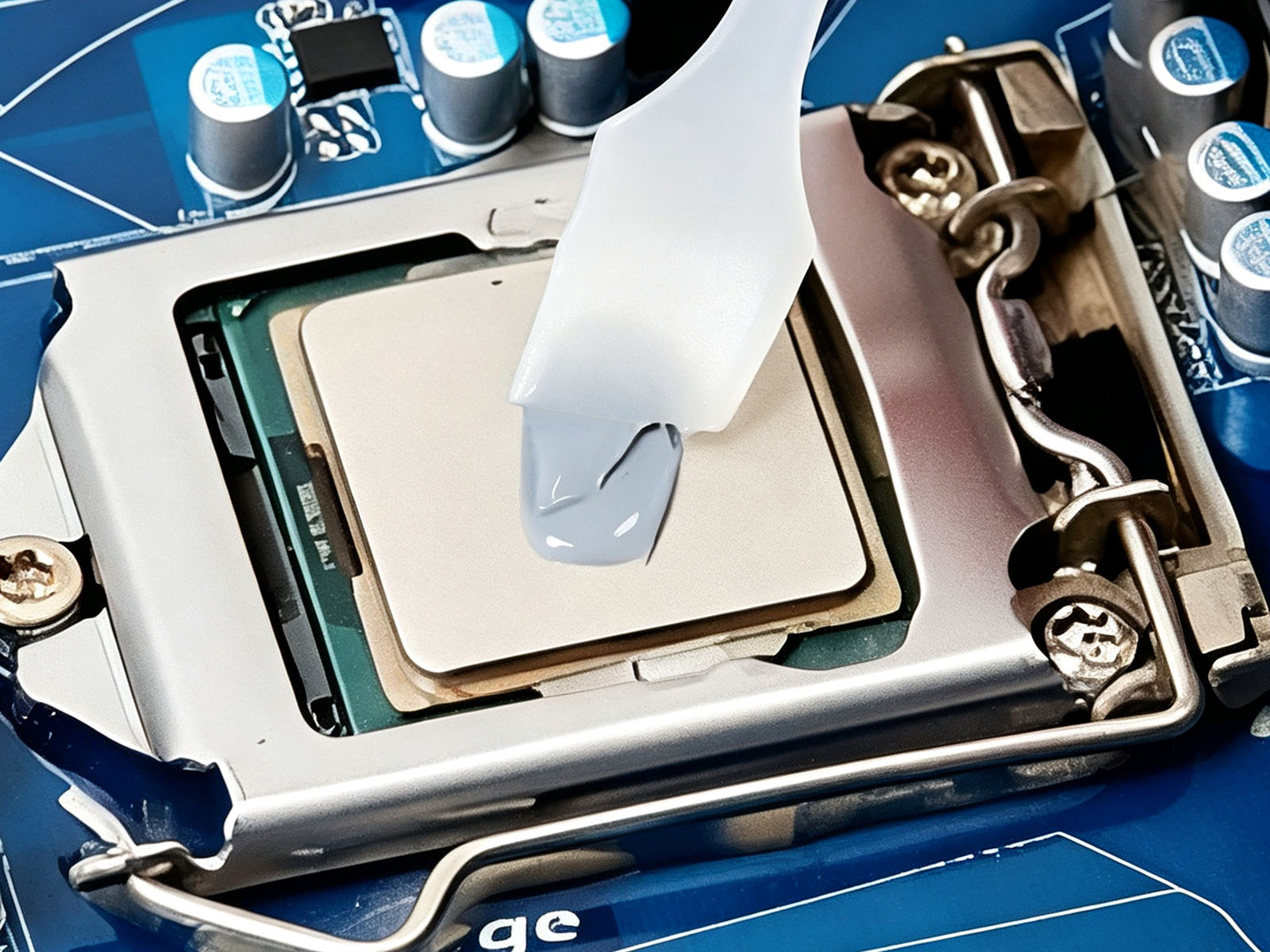
Chip Underfill
As microelectronic packaging technology continues to evolve toward higher integration and ultra-thin designs, advanced interconnection processes such as Flip Chip and Chip Scale Packaging (CSP) have become mainstream. However, the inherent coefficient of thermal expansion (CTE) mismatch between silicon chips and organic substrates causes interconnect solder balls to endure long-term alternating thermo-mechanical stresses during service, which easily leads to the initiation and propagation of fatigue cracks. Meanwhile, drop impacts and bending deformations experienced by portable devices also pose severe threats to the structural integrity of solder joints. To address these reliability challenges, Underfill technology has emerged.

OurKey Advantages
- Ultra-fast Capillary FlowIt can rapidly penetrate the tiny gaps of 50–100 μm beneath the chip via capillary action at room temperature, with minimal bubble formation during the filling process.
- Excellent Drop and Thermal Shock ResistanceAfter high-temperature reflow soldering, it maintains low residual stress, and during the instantaneous impact of drops in mobile phones and other devices, it effectively redistributes stress into the adhesive layer, significantly improving the drop-life of BGA/CSP solder joints.
- Broad Substrate Compatibility: It exhibits strong wetting and adhesion on common materials such as solder resist (green oil), copper pads (OSP, ENIG, tin-plated surfaces, etc.), and features low shrinkage upon curing, avoiding excessive compression on ultra-thin chips or low-dielectric constant materials.
Recommended Products

More Solutions
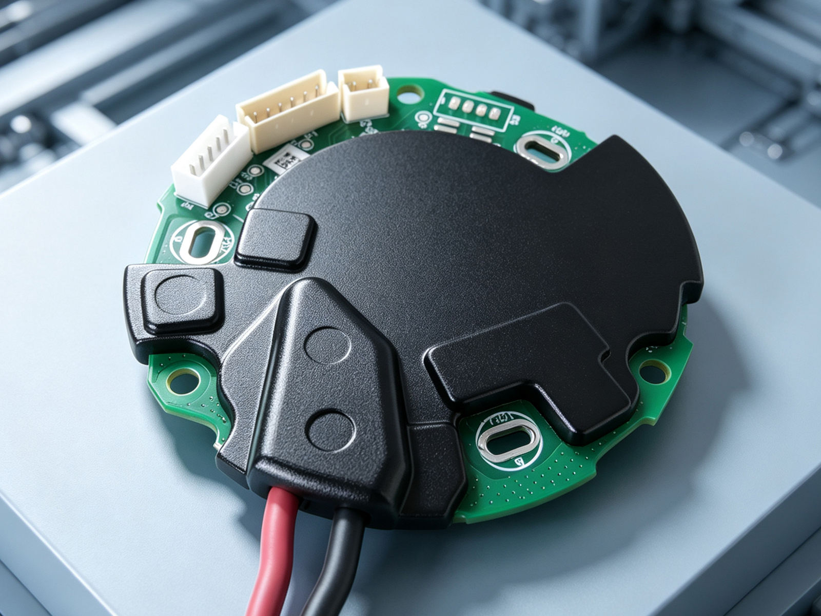
PCB Circuit Board Encapsulation Protection
View Details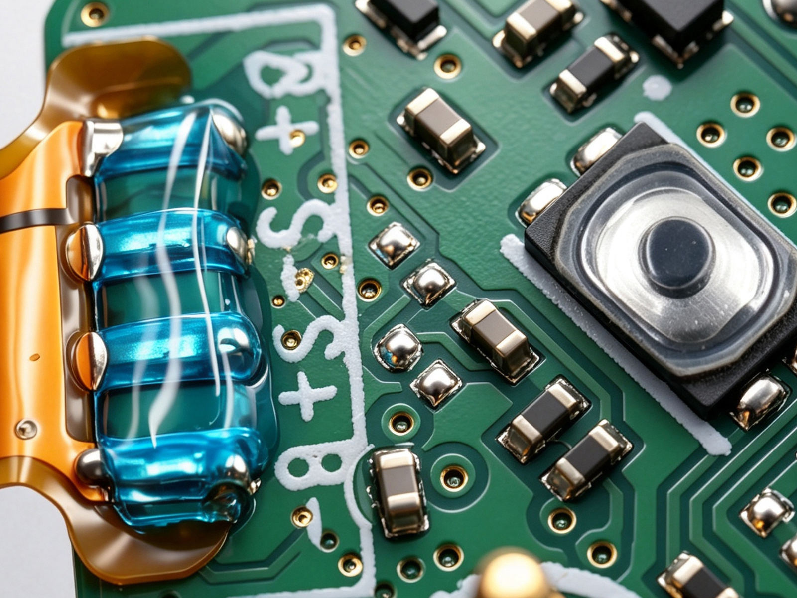
PIN Foot & Solder Joint Protection
View Details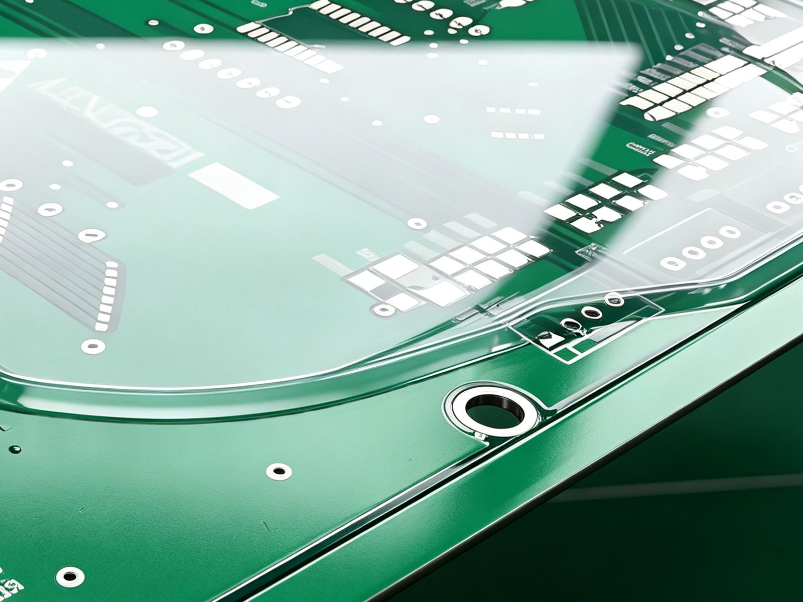
PCB Board Three-Proof Coating
View Details